
")
")
")
")
")
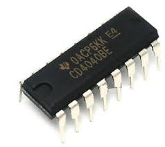
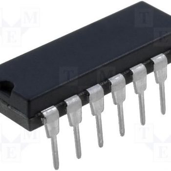
The CD4040 Binary Counter is a 12-stage ripple carry binary counter. The counters are advanced one counton the negative transition of each clock pulse. The counters are reset to the zero state by a logical “1” at thereset input independent of clock.The MC74C4040A is identical in pinout to the standard CMOS
MC14040. The device inputs are compatible with standard CMOSoutputs; with pullup resistors, they are compatible with LSTTLoutputs.This device consists of 12 master−slave flip−flops. The output ofeach flip−flop feeds the next and the frequency at each output is half ofthat of the preceding one. The state counter advances on thenegative−going edge of the Clock input. Reset is asynchronous andactive−high.State changes of the Q outputs do not occur simultaneously because
of internal ripple delays. Therefore, decoded output signals are subjectto decoding spikes and may have to be gated with the Clock of theHC4040A for some designs.
Features of CD4040 Binary Counter
• High Voltage Types (20V Rating)
• Medium Speed Operation
• Fully Static Operation
• Buffered Inputs and Outputs
• 100% Tested for Quiescent Current at 20V
• Standardized Symmetrical Output Characteristics
• Common Reset
• 5V, 10V and 15V Parametric Ratings
• Maximum Input Current of 1a at 18V Over Full Package-Temperature
Range;
– 100nA at 18V and 25oC
• Noise Margin (Over Full Package Temperature Range):
– 1V at VDD = 5V
– 2V at VDD = 10V
– 2.5V at VDD = 15V
• Output Drive Capability: 10 LSTTL Loads
• Outputs Directly Interface to CMOS, NMOS, and TTL
• Operating Voltage Range: 2.0 to 6.0 V
• Low Input Current: 1 A
• High Noise Immunity Characteristic of CMOS Devices
• In Compliance With JEDEC Standard No. 7A Requirements
• Chip Complexity: 398 FETs or 99.5 Equivalent Gates
• NLV Prefix for Automotive and Other Applications Requiring
Unique Site and Control Change Requirements; AEC−Q100
Qualified and PPAP Capable
• These Devices are Pb−Free, Halogen Free and are RoHS Compliant

Reviews
There are no reviews yet.