
")

")

")
")
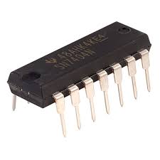
This device contains 7474 D Flip Flop two independent positive-edge-trig-gered D flip-flops with complementary outputs. The infor-mation on the D input is accepted by the flip-flops on the positive going edge of the clock pulse. The triggering occurs at a voltage level and is not directly related to the transition time of the rising edge of the clock. The data on the D input may be changed while the clock is LOW or HIGH without affecting the outputs as long as the data setup and hold times are not violated. A low logic level on the preset or clear inputs will set or reset the outputs regardless of the logic levels of the other inputs.
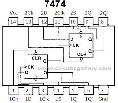
Features of 7474 D Flip Flop
- Recommended Voltage Supply Range:4.75-5.25V
- Maximum Supply Voltage:7V
- Maximum Input Voltage:7V
- Storage temperature : –65 to +150 °C
HIGH SPEED
fMAX = 71 MHz (TYP.) AT VCC =5V
. LOW POWER DISSIPATION
ICC = 2 µA (MAX.) AT TA = 25 °C
. HIGH NOISE IMMUNITY
VNIH = VNIL = 28 % VCC (MIN.)
. OUTPUT DRIVE CAPABILITY
10 LSTTL LOADS
. SYMMETRICAL OUTPUT IMPEDANCE
IOH = IOL = 4 mA (MIN.)
. BALANCED PROPAGATION DELAYS
tPLH = tPHL
. WIDE OPERATING VOLTAGE RANGE
VCC (OPR) = 2 V TO 6 V
. PIN AND FUNCTION COMPATIBLE
WITH 54/74LS74


Reviews
There are no reviews yet.