
")
")
")
")
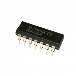
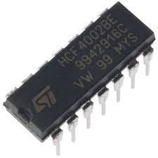
The 14042 Buffer Quad Transparent Latch is constructed with MOS P−channel and N−channel enhancement mode devices in a single monolithic structure. Each latch has a separate data input, but all four latches share a common clock. The clock polarity (high or low) used to strobe data through the latches can be reversed using the polarity
input. Information present at the data input is transferred to outputs Q and Q during the clock level which is determined by the polarity input. When the polarity input is in the logic “0” state, data is transferred during the low clock level, and when the polarity input is in the logic “1” state the transfer occurs during the high clock level

14042 Buffer Features:-
DC Supply Voltage Range: −0.5 to +18.0
Input or Output Voltage
Range (DC or Transient): −0.5 to VDD + 0.5
Input or Output Current
(DCorTransient) per Pin: ±10
Ambient Temperature Range: −55 to +125
Storage Temperature Range: −65 to +150
You can buy more product cheaper price from our shop FT232RL USB to UART Bridge, 24C256 EEPROM, etc
Reviews
There are no reviews yet.